
This dance, called
dynamic voltage and frequency scaling (DVFS), happens continually in the processor, called a system-on-chip (SoC), that runs your phone and your laptop as well as in the servers that back them. It’s all done in an effort to balance computational performance with power consumption, something that’s particularly challenging for smartphones. The circuits that orchestrate DVFS strive to ensure a steady clock and a rock-solid voltage level despite the surges in current, but they are also among the most backbreaking to design.
That’s mainly because the clock-generation and voltage-regulation circuits are analog, unlike almost everything else on your smartphone SoC. We’ve grown accustomed to a near-yearly introduction of new processors with substantially more computational power, thanks to advances in semiconductor manufacturing. “Porting” a digital design from an old semiconductor process to a new one is no picnic, but it’s nothing compared to trying to move analog circuits to a new process. The analog components that enable DVFS, especially a circuit called a low-dropout voltage regulator (LDO), don’t scale down like digital circuits do and must basically be redesigned from scratch with every new generation.
If we could instead build LDOs—and perhaps other analog circuits—from digital components, they would be much less difficult to port than any other part of the processor, saving significant design cost and freeing up engineers for other problems that cutting-edge chip design has in store. What’s more, the resulting digital LDOs could be much smaller than their analog counterparts and perform better in certain ways. Research groups in industry and academia have tested at least a dozen designs over the past few years, and despite some shortcomings, a commercially useful digital LDO may soon be in reach.
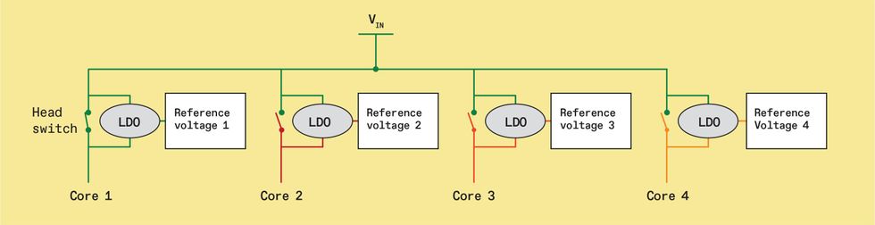
Low-dropout voltage regulators (LDOs) allow multiple processor cores on the same input voltage rail (VIN) to operate at different voltages according to their workloads. In this case, Core 1 has the highest performance requirement. Its head switch, really a group of transistors connected in parallel, is closed, bypassing the LDO and directly connecting Core 1 to VIN, which is supplied by an external power management IC. Cores 2 through 4, however, have less demanding workloads. Their LDOs are engaged to supply the cores with voltages that will save power.
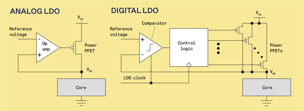
The basic analog low-dropout voltage regulator [left] controls voltage through a feedback loop. It tries to make the output voltage (VDD) equal to the reference voltage by controlling the current through the power PFET. In the basic digital design [right], an independent clock triggers a comparator [triangle] that compares the reference voltage to VDD. The result tells control logic how many power PFETs to activate.
A TYPICAL SYSTEM-ON-CHIP for a smartphone is a marvel of integration. On a single sliver of silicon it integrates multiple CPU cores, a graphics processing unit, a digital signal processor, a neural processing unit, an image signal processor, as well as a modem and other specialized blocks of logic. Naturally, boosting the clock frequency that drives these logic blocks increases the rate at which they get their work done. But to operate at a higher frequency, they also need a higher voltage. Without that, transistors can’t switch on or off before the next tick of the processor clock. Of course, a higher frequency and voltage comes at the cost of power consumption. So these cores and logic units dynamically change their clock frequencies and supply voltages—often ranging from 0.95 to 0.45 volts— based on the balance of energy efficiency and performance they need to achieve for whatever workload they are assigned—shooting video, playing back a music file, conveying speech during a call, and so on.
Typically, an external power-management IC generates multiple input voltage (VIN) values for the phone’s SoC. These voltages are delivered to areas of the SoC chip along wide interconnects called rails. But the number of connections between the power-management chip and the SoC is limited. So, multiple cores on the SoC must share the same VIN rail.
But they don’t have to all get the same voltage, thanks to the low-dropout voltage regulators. LDOs along with dedicated clock generators allow each core on a shared rail to operate at a unique supply voltage and clock frequency. The core requiring the highest supply voltage determines the shared VIN value. The power-management chip sets VIN to this value and this core bypasses the LDO altogether through transistors called head switches.
To keep power consumption to a minimum, other cores can operate at a lower supply voltage. Software determines what this voltage should be, and analog LDOs do a pretty good job of supplying it. They are compact, low cost to build, and relatively simple to integrate on a chip, as they do not require large inductors or capacitors.
But these LDOs can operate only in a particular window of voltage. On the high end, the target voltage must be lower than the difference between VIN and the voltage drop across the LDO itself (the eponymous “dropout” voltage). For example, if the supply voltage that would be most efficient for the core is 0.85 V, but VIN is 0.95 V and the LDO’s dropout voltage is 0.15 V, that core can’t use the LDO to reach 0.85 V and must work at the 0.95 V instead, wasting some power. Similarly, if VIN has already been set below a certain voltage limit, the LDO’s analog components won’t work properly and the circuit can’t be engaged to reduce the core supply voltage further.
The main obstacle that has limited use of digital LDOs so far is the slow transient response.
However, if the desired voltage falls inside the LDO’s window, software enables the circuit and activates a reference voltage equal to the target supply voltage.
HOW DOES THE LDO supply the right voltage? In the basic analog LDO design, it’s by means of an operational amplifier, feedback, and a specialized power p-channel field effect transistor (PFET). The latter is a transistor that reduces its current with increasing voltage to its gate. The gate voltage to this power PFET is an analog signal coming from the op amp, ranging from 0 volts to VIN. The op amp continuously compares the circuit’s output voltage—the core’s supply voltage, or VDD—to the target reference voltage. If the LDO’s output voltage falls below the reference voltage—as it would when newly active logic suddenly demands more current—the op amp reduces the power PFET’s gate voltage, increasing current and lifting VDD toward the reference voltage value. Conversely, if the output voltage rises above the reference voltage—as it would when a core’s logic is less active—then the op amp increases the transistor’s gate voltage to reduce current and lower VDD.
A basic
digital LDO, on the other hand, is made up of a voltage comparator, control logic, and a number of parallel power PFETs. (The LDO also has its own clock circuit, separate from those used by the processor core.) In the digital LDO, the gate voltages to the power PFETs are binary values instead of analog, either 0 V or VIN.
With each tick of the clock, the comparator measures whether the output voltage is below or above the target voltage provided by the reference source. The comparator output guides the control logic in determining how many of the power PFETs to activate. If the LDO’s output is below target, the control logic will activate more power PFETs.Their combined current props up the core’s supply voltage, and that value feeds back to the comparator to keep it on target. If it overshoots, the comparator signals to the control logic to switch some of the PFETs off.
NEITHER THE ANALOG nor the digital LDO is ideal, of course. The key advantage of an analog design is that it can respond rapidly to transient droops and overshoots in the supply voltage, which is especially important when those events involve steep changes. These transients occur because a core’s demand for current can go up or down greatly in a matter of nanoseconds. In addition to the fast response, analog LDOs are very good at suppressing variations in VIN that might come in from the other cores on the rails. And, finally, when current demands are not changing much, it controls the output tightly without constantly overshooting and undershooting the target in a way that introduces ripples in VDD.
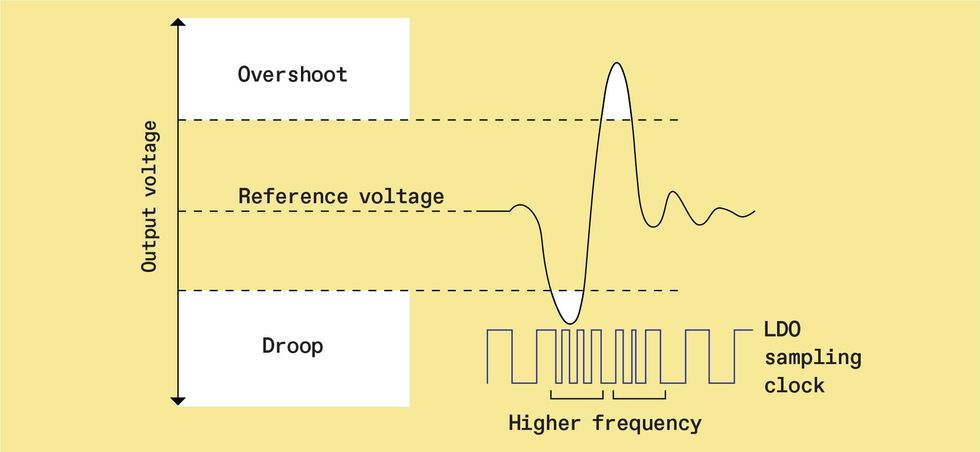
When a core’s current requirement changes suddenly it can cause the LDO’s output voltage to overshoot or droop [top]. Basic digital LDO designs do not handle this well [bottom left]. However, a scheme called adaptive sampling with reduced dynamic stability [bottom right] can reduce the extent of the voltage excursion. It does this by ramping up the LDO’s sample frequency when the droop gets too large, allowing the circuit to respond faster.
Source: S.B. Nasir et al., IEEE International Solid-State Circuits Conference (ISSCC), February 2015, pp. 98–99.
These attributes have made analog LDOs attractive not just for supplying processor cores, but for almost any circuit demanding a quiet, steady supply voltage. However, there are some critical challenges that limit the effectiveness of these designs. First analog components are much more complex than digital logic, requiring lengthy design times to implement them in advanced technology nodes. Second, they don’t operate properly when VIN is low, limiting how low a VDD they can deliver to a core. And finally, the dropout voltage of analog LDOs isn’t as small as designers would like.
Taking those last points together, analog LDOs offer a limited voltage window at which they can operate. That means there are missed opportunities to enable LDOs for power saving—ones big enough to make a noticeable difference in a smartphone’s battery life.
Digital LDOs undo many of these weaknesses: With no complex analog components, they allow designers to tap into a wealth of tools and other resources for digital design. So scaling down the circuit for a new process technology will need much less effort. Digital LDOs will also operate over a wider voltage range. At the low-voltage end, the digital components can operate at VIN values that are off-limits to analog components. And in the higher range, the digital LDO’s dropout voltage will be smaller, resulting in meaningful core-power savings.
But nothing’s free, and the digital LDO has some serious drawbacks. Most of these arise because the circuit measures and alters its output only at discrete times, instead of continuously. That means the circuit has a comparatively slow response to supply voltage droops and overshoots. It’s also more sensitive to variations in VIN, and it tends to produce small ripples in the output voltage, both of which could degrade a core’s performance.
Of these, the main obstacle that has limited the use of digital LDOs so far is their slow transient response. Cores experience droops and overshoots when the current they draw abruptly changes in response to a change in its workload. The LDO response time to droop events is critical to limiting how far voltage falls and how long that condition lasts. Conventional cores add a safety margin to the supply voltage to ensure correct operation during droops. A greater expected droop means the margin must be larger, degrading the LDO’s energy-efficiency benefits. So, speeding up the digital LDO’s response to droops and overshoots is the primary focus of the cutting-edge research in this field.
SOME RECENT ADVANCES have helped speed the circuit’s response to droops and overshoots. One approach uses the digital LDO’s clock frequency as a control knob to trade stability and power efficiency for response time.
A lower frequency improves LDO stability, simply because the output will not be changing as often. It also lowers the LDO’s power consumption, because the transistors that make up the LDO are switching less frequently. But this comes at the cost of a slower response to transient current demands from the processor core. You can see why that would be, if you consider that much of a transient event might occur within a single clock cycle if the frequency is too low.
Conversely, a high LDO clock frequency reduces the transient response time, because the comparator is sampling the output often enough to change the LDO’s output current earlier in the transient event. However, this constant sampling degrades the stability of the output and consumes more power.
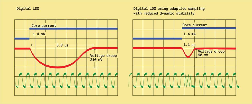
The gist of this approach is to introduce a clock whose frequency adapts to the situation, a scheme called adaptive sampling frequency with reduced dynamic stability. When voltage droops or overshoots exceed a certain level, the clock frequency increases to more rapidly reduce the transient effect. It then slows down to consume less power and keep the output voltage stable. This trick is achieved by adding a pair of additional comparators to sense the overshoot and droop conditions and trigger the clock. In measurements from a test chip using this technique, the VDD droop reduced from 210 to 90 millivolts—a 57 percent reduction versus a standard digital LDO design. And the time it took for voltage to settle to a steady state shrank to 1.1 microseconds from 5.8 µs, an 81 percent improvement.
An alternative approach for improving the transient response time is to make the digital LDO a little bit analog. The design integrates a separate analog-assisted loop that responds instantly to load current transients. The analog-assisted loop couples the LDO’s output voltage to the LDO’s parallel PFETs through a capacitor, creating a feedback loop that engages only when there is a steep change in output voltage. So, when the output voltage droops, it reduces the voltage at the activated PFET gates and instantaneously increases current to the core to reduce the magnitude of the droop. Such an analog-assisted loop has been shown to reduce the droop from 300 to 106 mV, a 65 percent improvement, and overshoot from 80 to 70 mV (13 percent).
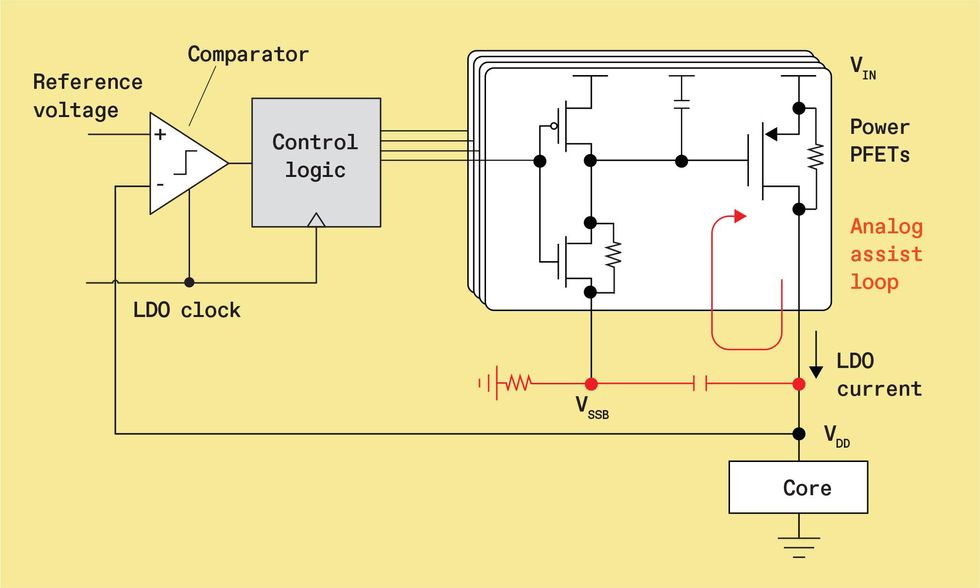

An alternative way to make digital LDOs respond more quickly to voltage droops is to add an analog feedback loop to the power PFET part of the circuit [top]. When output voltage droops or overshoots, the analog loop engages to prop it up [bottom], reducing the extent of the excursion.
Source: M. Huang et al., IEEE Journal of Solid-State Circuits, January 2018, pp. 20–34.
Of course, both of these techniques have their drawbacks. For one, neither can really match the response time of today’s analog LDOs. In addition, the adaptive sampling frequency technique requires two additional comparators and the generation and calibration of reference voltages for droop and overshoot, so the circuit knows when to engage the higher frequency. The analog-assisted loop includes some analog components, reducing the design-time benefit of an all-digital system.
Developments in commercial SoC processors may help make digital LDOs more successful, even if they can’t quite match analog performance. Today, commercial SoC processors integrate all-digital adaptive circuits designed to mitigate performance problems when droops occur. These circuits, for example, temporarily stretch the core’s clock period to prevent timing errors. Such mitigation techniques could relax the transient response-time limits, allowing the use of digital LDOs and boosting processor efficiency. If that happens, we can expect more efficient smartphones and other computers, while making the process of designing them a whole lot easier.